
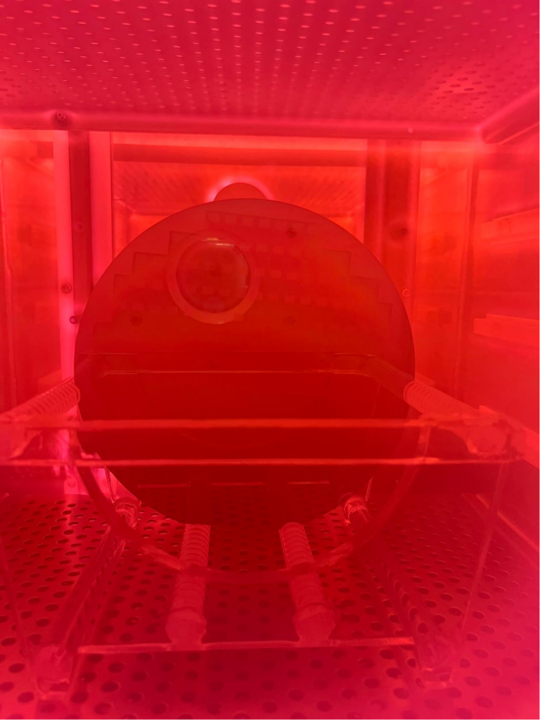
At wafer scale, contamination does not need to be visible to become a yield problem.
Trace grinding wax, handling oil, photoresist residue and other organic contamination can remain after cutting, grinding, lithography or previous wet-cleaning steps. When those residues survive into bonding, deposition, die attach or dispensing, they can interfere with the interface that the next process depends on.
That is why plasma treatment for semiconductor processing is increasingly used as a precision surface-preparation step rather than simply another general cleaning method.
Modern semiconductor manufacturing gives contamination less room to hide and less tolerance to remain.
Micron- and sub-micron-scale structures can retain residues that are difficult to remove consistently with bulk liquid cleaning alone. At the same time, aggressive chemical cleaning can create its own challenges when a wafer or surface structure is sensitive to liquids, residues or excessive material removal.
The issue is especially relevant in advanced packaging, Mini-LED, power semiconductor manufacturing and third-generation semiconductor materials such as SiC and GaN.
Depending on the gas chemistry and process recipe, wafer plasma cleaning is commonly used to address:
For a broader explanation of the mechanism, see our guide to plasma cleaning technology.
Inside a controlled vacuum chamber, process gas is energized to form plasma. Reactive species interact with contamination on the exposed wafer surface.
The exact effect depends strongly on gas composition, power, pressure and exposure time.
Oxygen-containing plasma is commonly used for organic removal and resist-related applications, while other gases can provide different chemical or physical surface effects.
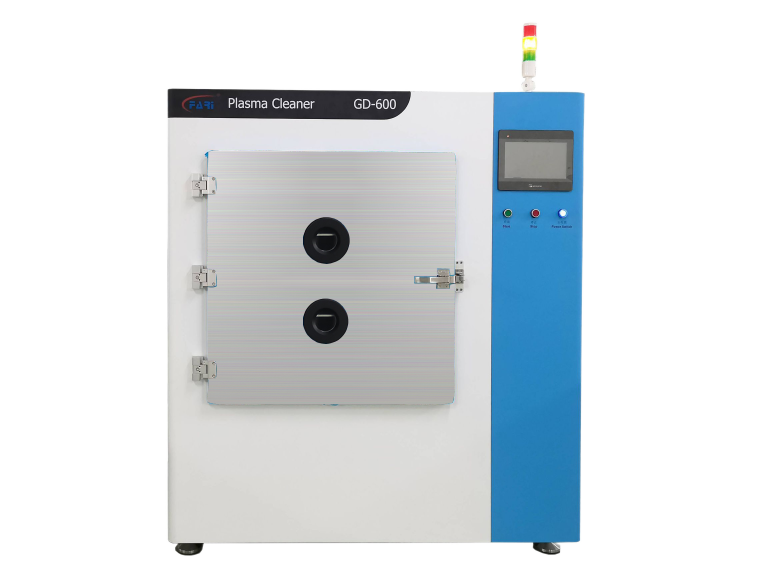
A system such as the GD-10RF compact RF O2 plasma cleaner provides RF power and controlled gas delivery for laboratory and small-batch process development.
Plasma adds no liquid cleaning bath to the treatment step. Reactive products generated during cleaning can be removed through the vacuum system.
This makes it useful when liquid residue, drying or water marks are undesirable.
Plasma can access exposed microstructures, grooves and recessed features without relying on a liquid to wet, rinse and dry each feature correctly.
Fixture design and plasma distribution still matter, especially on complex structures, but the process provides a useful option for difficult-to-clean geometries.
Removing residue is only part of the objective. Plasma treatment can also change the surface condition and increase wettability for compatible downstream materials.
This can support processes such as bonding, coating, die attach, underfill and dispensing when the interface needs both cleanliness and controlled surface energy.
Low-temperature plasma can be useful for thin wafers, epitaxial wafers and temperature-sensitive substrates because the purpose is surface treatment rather than bulk heating.
The process still needs to be validated against the exact wafer, film stack and device structure.
Plasma should not be described as a universal replacement for wet cleaning.
Wet cleaning remains important for high-volume semiconductor processing and many types of inorganic contamination. Plasma is particularly useful where a dry finishing step, organic residue removal or surface activation is required immediately before the next process.
Typical positions include:
For packaging-related applications, also see our guide to vacuum plasma cleaning for semiconductor chips and advanced packaging.
Yes, but uniformity depends on equipment design rather than the word “plasma” alone.
The chamber, electrode layout, carrier and wafer position all need to match the wafer diameter. As substrate size increases, differences between the wafer center and edge become more important during process development.
A production process should therefore be qualified across the entire usable wafer area rather than evaluated from a single measurement point.
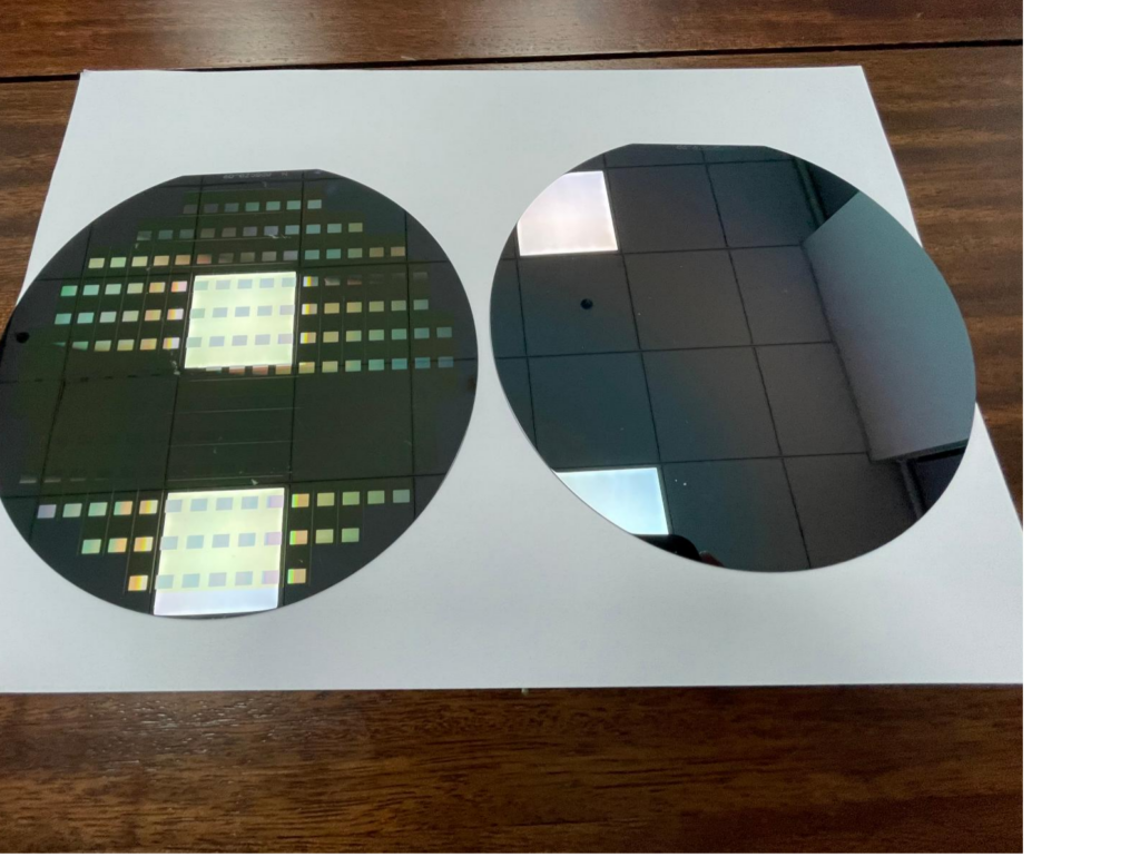
Low thermal loading makes plasma attractive for thin substrates, but mechanical handling becomes more important as wafer thickness decreases.
Dedicated carriers or fixtures should support the wafer during loading, pumping, treatment and unloading so that a surface-cleaning process does not introduce mechanical damage elsewhere.
Silicon carbide and gallium nitride substrates can also be processed with plasma, but gas chemistry and plasma dose must be developed specifically for the substrate and downstream objective.
Applications can include organic residue removal and surface preparation before selected etching, bonding or deposition operations.
A recipe qualified for silicon should not automatically be transferred to SiC or GaN without process validation.
Plasma processes can be configured for controlled surface modification or light oxide-related treatment, but thick oxide removal is a different requirement from ordinary organic cleaning.
If substantial SiO2 removal is required, the process should be evaluated as an etching application rather than assuming a standard cleaning recipe will provide sufficient removal rate.
A freshly plasma-treated wafer has an activated surface that can gradually change during exposure to ambient air.
Organic molecules can be re-adsorbed and surface energy can decrease over time. For critical bonding, coating or dispensing operations, the next process should therefore follow plasma cleaning as soon as the manufacturing flow allows.
No. The two methods solve different problems and are often complementary. Wet cleaning is well established for many bulk and chemical-cleaning steps, while plasma is particularly useful for dry fine cleaning, organic residue removal and surface activation.
A properly developed low-damage recipe is intended to modify only the required surface layer. Gas chemistry, RF power, bias, exposure time, film stack and substrate type must still be validated for each process.
Oxygen-based plasma is widely used for organic resist-related processes. The required recipe depends on whether the goal is light descum, residual organic removal or full resist ashing.
Yes, but the process should be tuned for the specific compound semiconductor, existing films and desired surface result.
Start with the wafer material, diameter, contamination type and downstream process rather than selecting power and treatment time in isolation.
If you need a plasma process for silicon, SiC, GaN, epitaxial wafers or advanced packaging, contact FARI Plasma with your wafer size, process step and contamination target.



English

Spanish
Rogatus ad ultimum admissusque in consistorium ambage nulla praegressa inconsiderate