
By Fari Plasma Applications Engineering | Reviewed March 2026
A mid-sized consumer electronics manufacturer in Southeast Asia replaced its isopropyl alcohol wipe step with inline atmospheric plasma treatment and cut bonding-related scrap from 8.2% to 5.4% in six weeks — a 34% reduction that paid back the equipment cost in six months. The root cause wasn’t exotic: a solvent wipe left silicone residues and inconsistent surface energy on plastic housings, and no amount of operator retraining was going to fix a chemistry problem. Plasma fixed it by activating the surface at the molecular level, right before the adhesive dispenser, every single time.
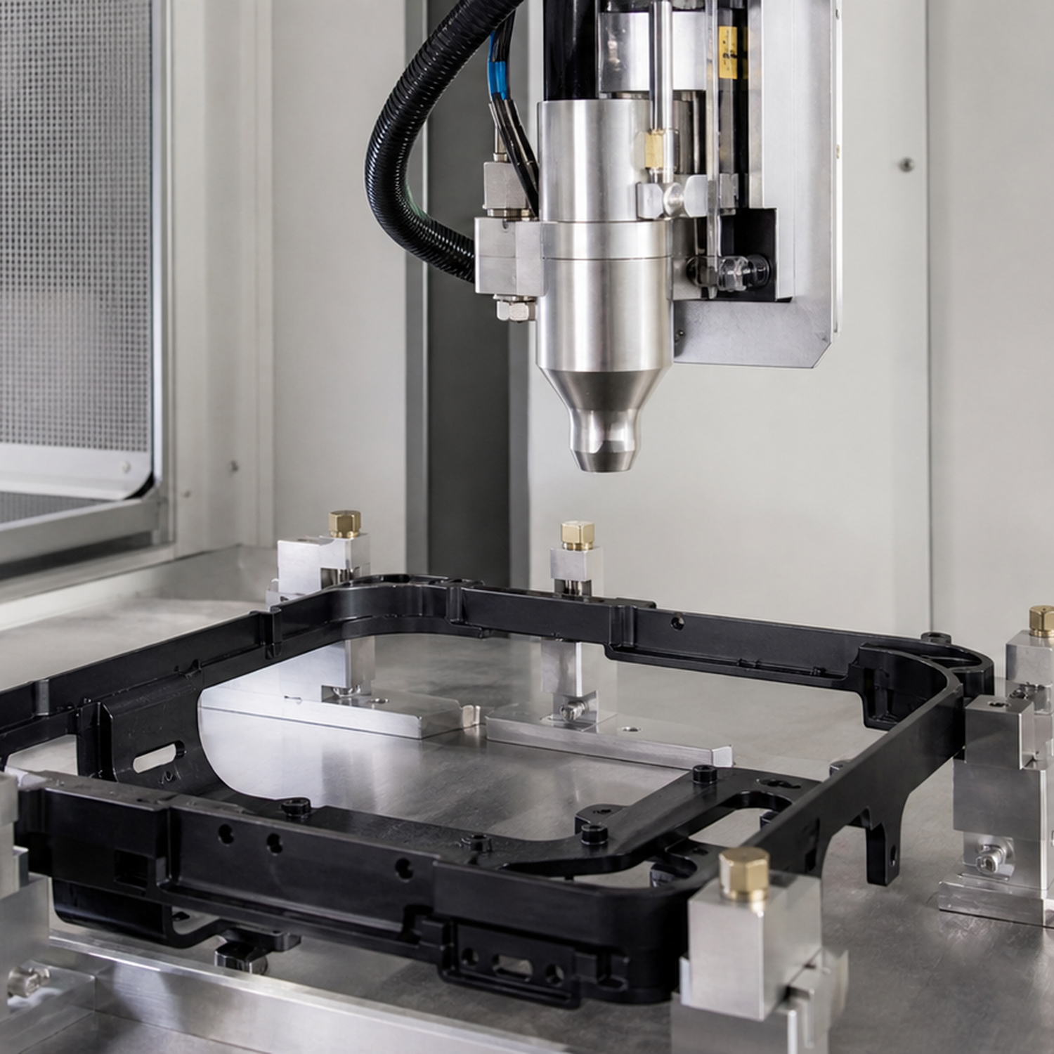
Two plasma delivery methods cover most electronics assembly work. Atmospheric plasma runs at ambient pressure, integrates directly into a moving conveyor line, and treats parts in seconds — well suited to continuous, high-volume production with consistent part geometry, like the housings in this case. Vacuum plasma treats a batch of parts inside a sealed, evacuated chamber, giving more uniform coverage on complex 3D shapes and recessed features, but requiring a load/pump-down/vent cycle that fits high-mix or lower-volume work better than a fast-moving line. Neither is universally “better” — the choice depends on part geometry, volume, and how much floor space a line has near the bonding or coating step.
The manufacturer produced roughly 180,000 units per month of a wearable device: a polycarbonate top housing bonded to an ABS base with a two-part structural acrylic adhesive. Roughly 14,760 units a month — 8.2% of output — failed either the on-floor shear test or came back from distributors with delaminated seams. Engineering had already tightened adhesive dispense volume, validated cure oven uniformity, and swapped adhesive suppliers twice. Scrap crept down a point, then crept back up.
The variable nobody had instrumented properly was the surface itself. A manual IPA wipe, applied about 40 seconds before adhesive dispense, looked clean and smelled clean — it wasn’t. IPA removes loose dust and fingerprints, but it also redistributes low-surface-energy contaminants like silicone mold-release residue rather than removing them. That’s a common failure point across electronics assembly: low surface energy is invisible to a visual inspection but fatal to a structural bond. Air, oxygen, nitrogen, and argon each strip different residues and raise surface energy through different mechanisms — see the Plasma Gas Selection Guide: Air, O2, N2, Ar.
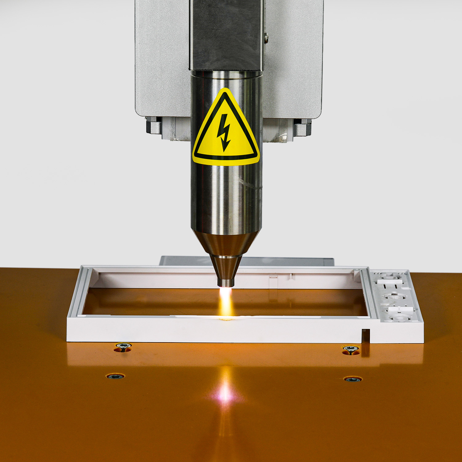
Plasma surface activation raises surface energy by oxidizing the outermost molecular layer, giving adhesives, coatings, and inks something to actually bond to instead of beading up. That’s the mechanism at play here — surface activation for adhesive bonding, distinct from the etching or photoresist ashing used further upstream in semiconductor packaging: Plasma Ashing & Photoresist Removal. Which of the three mechanisms applies to a given defect depends on what’s actually failing — the activation vs. cleaning vs. etching split.
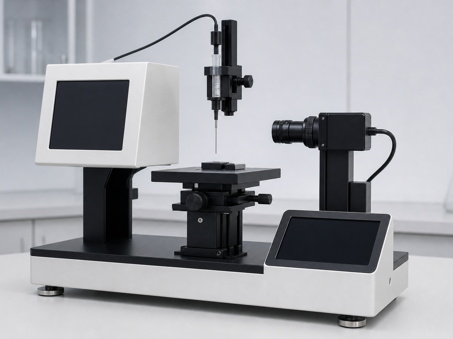
Housings moved from injection molding to a manual IPA wipe station, then straight to adhesive dispense. The plant’s senior process engineer ran a two-week surface audit, pulling 50 post-wipe housings for dyne ink vs. contact angle vs. XPS testing. Surface energy ranged from 32 to 44 dyne/cm — under the adhesive’s 52 dyne/cm minimum — with two units showing silicone contamination traced to the molder’s release agent. Contact angle with deionized water swung from 68° to 91° depending on which operator wiped the part.
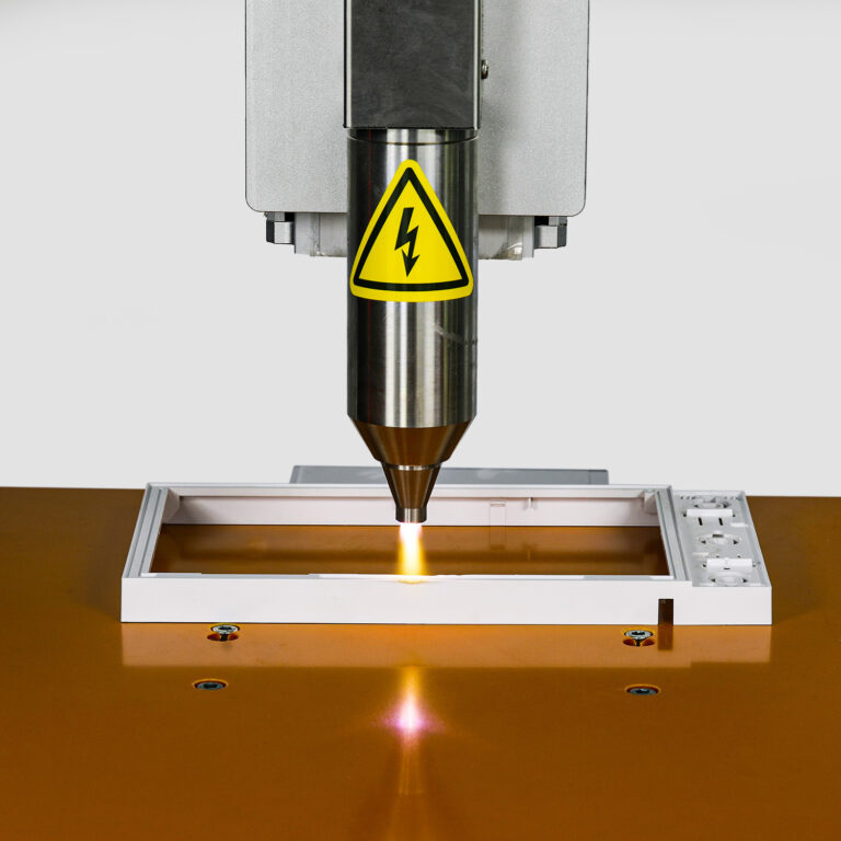
A rotary atmospheric plasma nozzle was mounted 55 cm upstream of the adhesive dispenser, fed with filtered compressed dry air and gated by a PLC tap on the conveyor encoder so it only fired when a part was present. The same engineer ran a two-day DOE and set the line at 380 W, an 8 mm treatment distance, and a 120 mm/s traverse speed matched to conveyor speed — adding 2.3 seconds of treatment time per unit with no batching or pump-down delay. Post-treatment surface energy stabilized at 68–72 dyne/cm, validated with dyne inks every 500 units and cross-checked with contact angle measurement after plasma treatment.
| Metric | Before Plasma | After Plasma |
|---|---|---|
| Bonding-related scrap rate | 8.2% | 5.4% |
| Defective units per month | 14,760 | 9,720 |
The gap works out to 5,040 fewer scrap units a month. At a fully-loaded unit cost of $9.40, that’s $47,376/month in avoided scrap cost, plus $4,400/month saved by eliminating IPA and wipe consumables — a combined $51,776/month against a capital and integration cost of roughly $310,000. Simple payback: 6.0 months.
The residual 5.4% scrap is worth noting: plasma resolved the adhesion-driven failures, not cosmetic defects, dimensional issues, or electrical test failures. It’s a surface tool, not a universal fix.
Bonding two plastic housings is one failure mode among several that respond to the same fix. PCB assembly lines commonly run into flux residue on pads and vias that blocks conformal coating from wetting evenly — an oxygen-based plasma pass ahead of coating removes it without solvent chemistry, using the same O2 plasma options suited to organic residue removal. Wire bonding faces a parallel problem: thin oxide layers and organic films on bond pads reduce pull strength and increase lift rates, and a brief plasma pass ahead of bonding raises yield the same way it raised bond strength on this housing. Substrate and volume both drive method selection for these PCB and semiconductor-adjacent applications: PCB plasma cleaning.
If your scrap signature includes delamination, coating lift, or ink rub-off — and your parts currently get a solvent wipe, flame treatment, or corona pass with high unit-to-unit variance — the pattern above likely applies. Silicone mold-release residue and low surface energy are common across injection-molded consumer electronics housings regardless of geometry, and assemblies combining plastics and rubber components often show the widest surface energy spread before treatment and the biggest relative improvement after.
The lesson transfers across substrates and industries. A Tier 1 automotive supplier working through similar bond-strength issues added an inline plasma step and eliminated primer coats on a Tier 1 line entirely — see Eliminate Primer Coats with Inline Plasma. A medical device manufacturer facing rejection-related scrap from adhesion and coating failures cut rejections 40% using the same underlying mechanism on a different substrate — plasma treatment medical device case.
Plasma isn’t a drop-in fix for every scrap problem. Line integration adds a process step and a validation window — expect a short DOE to find the right power, speed, and distance for your substrate. Effectiveness depends on matching gas chemistry to contaminant type; compressed air worked here, but other contaminants and oxides respond better to different gases, covered in the gas selection guide linked above. Activation also decays: this line measured meaningful decay within 4 hours on polycarbonate at 45% RH, well short of the nozzle supplier’s “up to 72 hours” claim, so bonding has to happen inside a validated window, not whenever the schedule allows. And root-cause analysis still matters — if defects aren’t adhesion-related, plasma options like activation, cleaning, or etching won’t move the number. Before scoping integration costs, a system cost breakdown is a reasonable starting point.
Ask three questions before investing further: Is a meaningful share of your defects adhesion-related? Are you seeing high unit-to-unit variance from a solvent wipe, flame, or corona process? Do you have 30–60 cm of conveyor space near the bonding or coating step? Two yeses out of three usually means the math works. The plasma system supplier catalog lists both catalog and OEM/ODM configurations for teams ready to scope a line. To sanity-check a specific substrate, adhesive, or volume against a similar project, reach out through Contact Us — a feasibility review is the fastest way to know if this applies to you.
What are the disadvantages of plasma treatment?
Line integration adds a process step and validation time. Effectiveness depends on matching gas and dose to the specific contaminant, and consistent fixture or part positioning is required for repeatable results. Not every defect is adhesion-related, so root-cause analysis still matters before assuming plasma will fix a scrap problem.
How long does the plasma treatment last?
Surface activation decays over time — this case measured meaningful decay within about 4 hours on polycarbonate at 45% relative humidity, though decay rate varies by material and environment. Bonding or coating should happen within a validated window after treatment, not days later, so timing needs testing on the actual substrate.
What is the best plasma treatment for electronics assembly?
There’s no single best method — it depends on material, contamination type, and whether an inline atmospheric system or a batch vacuum chamber fits the production line’s throughput and geometry. Substrate and volume both drive that choice more than any general ranking of methods.
What equipment is used for plasma surface treatment in electronics manufacturing?
Common options include benchtop plasma cleaners for lab or pilot runs, inline atmospheric plasma systems for continuous production, and vacuum plasma chambers for batch processing that needs deeper, more uniform treatment across complex geometries.



English

Spanish
Rogatus ad ultimum admissusque in consistorium ambage nulla praegressa inconsiderate